

 Colored
 Grayscale
SEM excels in detailed surface imaging, morphology, and elemental composition, making it ideal for examining microstructures, coatings, and topography of a wide range of solid materials. Unlike TEM, which reveals internal structures, or AFM, which maps surface properties in 3D, Scanning Electron Microscopy (SEM) provides high-resolution, depth-rich images of sample surfaces.
The best choice between SEM and other microscopy techniques depends on your sample’s characteristics and the information you seek.
| Surface Morphology & Texture | Moderately Robust & Conductive Samples | High Magnification & Depth of Field | Elemental Analysis with EDS |
| Perfect for analyzing cracks, roughness, coatings, and structural patterns at micro to nanoscale. | Ideal for metals, minerals, ceramics, polymers, and biological specimens with conductive coatings. | Produces crisp, 3D-like images with exceptional clarity and spatial awareness. | Combines with Energy Dispersive X-ray Spectroscopy for identifying surface chemical composition. |
Our Work & Results
We proudly showcase the high-resolution imaging and surface analysis achieved through Scanning Electron Microscopy (SEM) at the Nanoscopy Science Center. Our work highlights SEM’s ability to reveal detailed surface structures and compositions at the microscale and nanoscale, advancing research across materials science, biology, and engineering.
Image 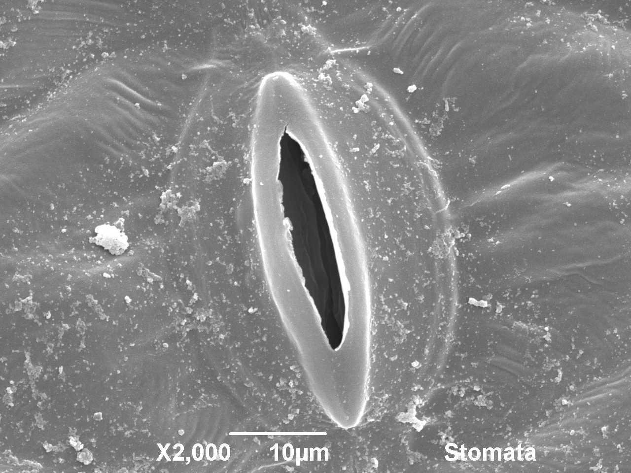 | Image 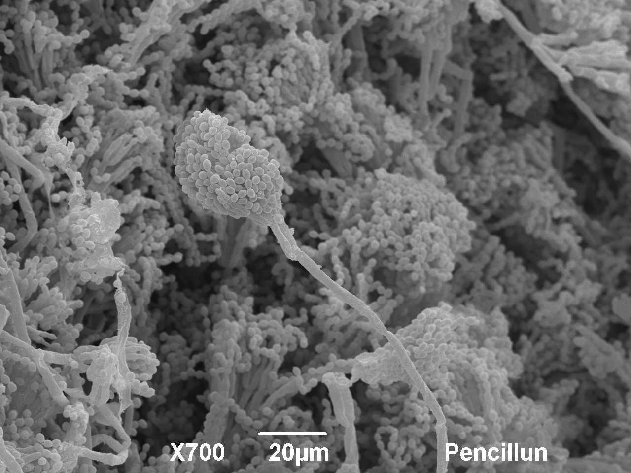 | Image 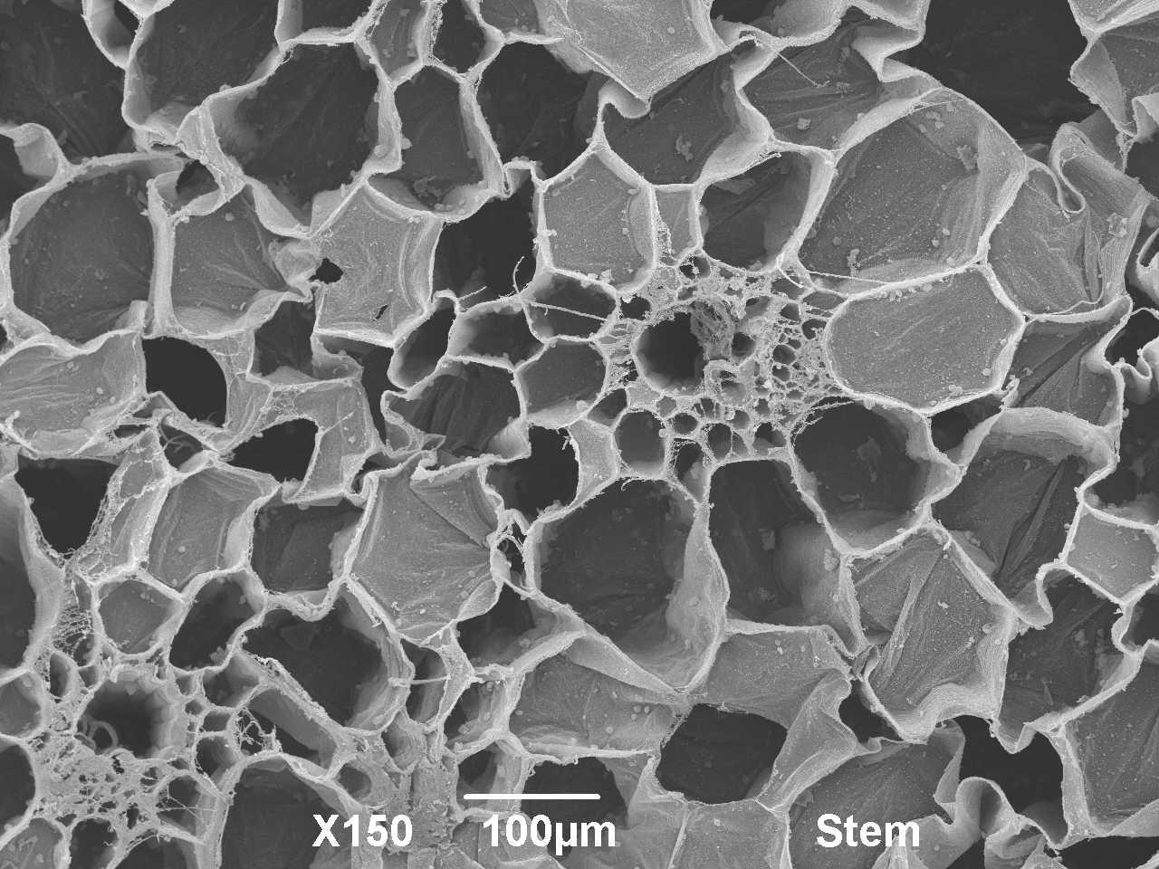 |
Image 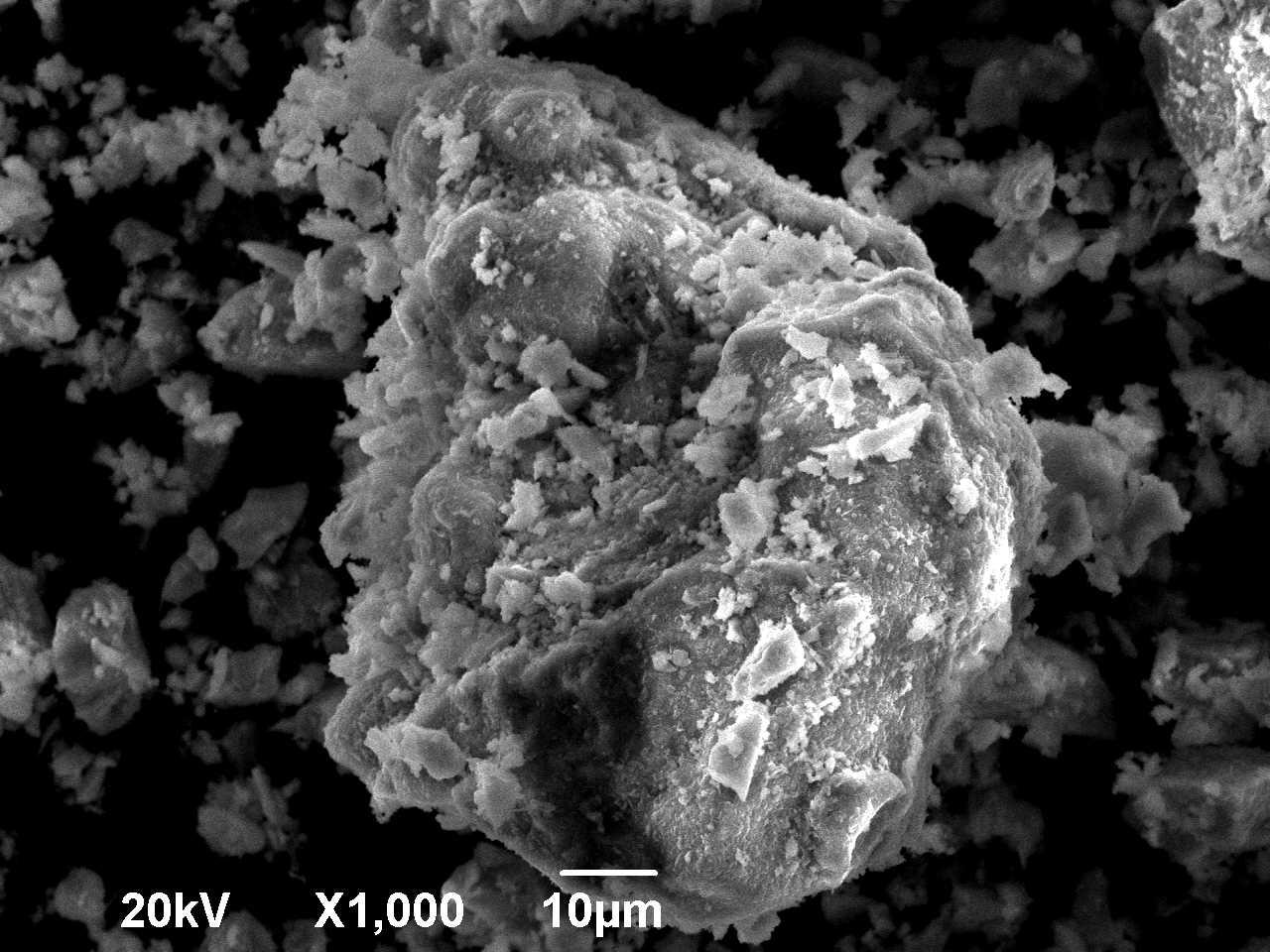 | Image 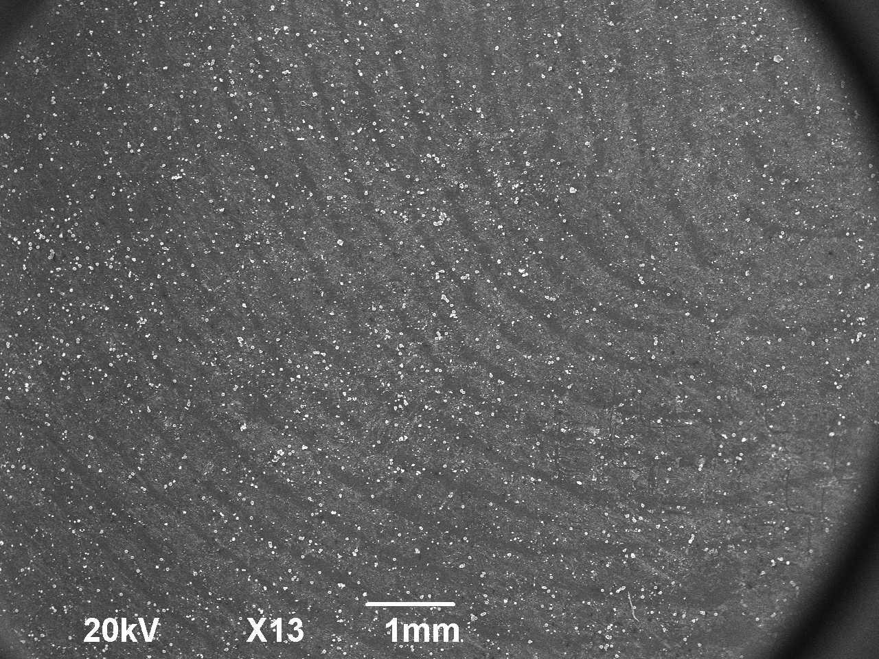 | Image 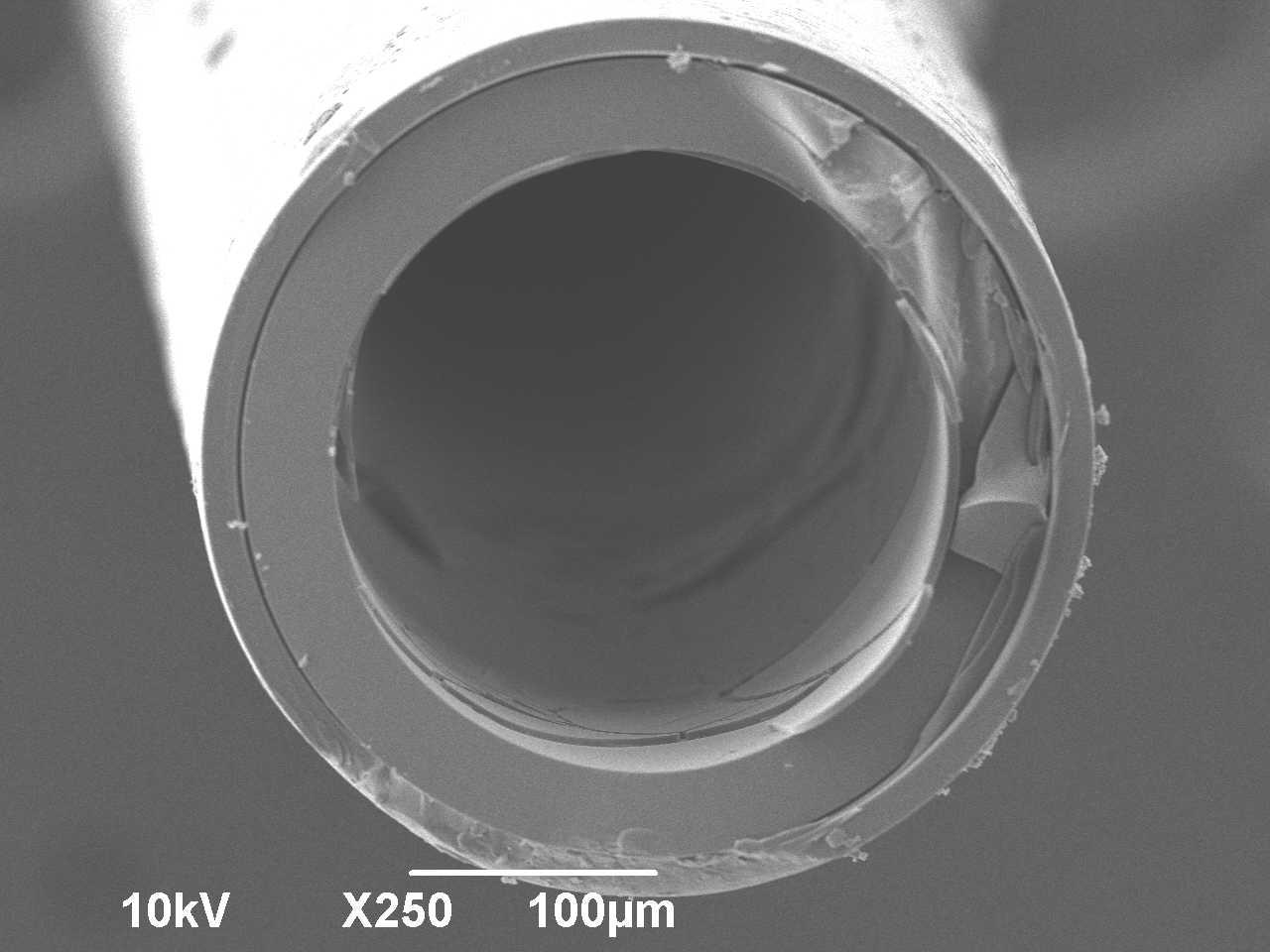 |
Ready to Explore the Nanoscale?
Apply now to access cutting-edge imaging technologies at the Nanoscopy Science Center. Whether you're working with biological samples or advanced materials, our expert team and state-of-the-art instruments are here to support your research. Submit your application here.