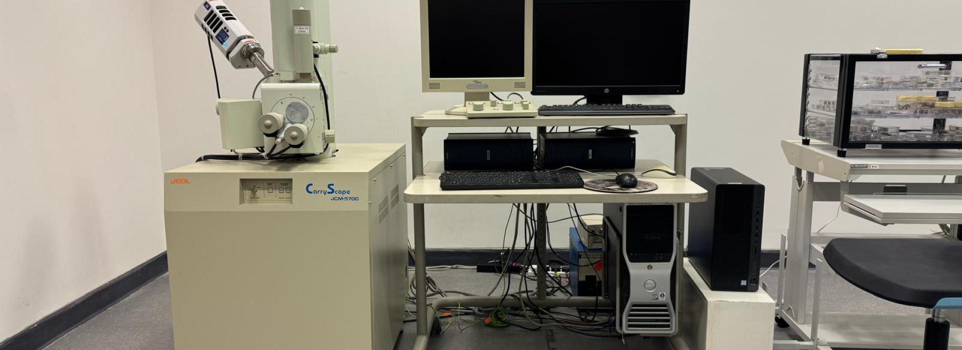
Scanning Electron Microscope
Our JEOL JCM-5700 Scanning Electron Microscope (SEM) is engineered for advanced surface characterization and high-resolution imaging. This instrument delivers:
- Exceptional Spatial Resolution: Achieves nanometer-scale resolution, enabling the detailed visualization of surface morphology and topography.
- Broad Magnification Range: Provides continuous magnification from 10x to 300,000x, facilitating comprehensive analysis from macroscopic features to ultrafine structures.
- Variable Accelerating Voltage: Electron beam acceleration is adjustable from 0.5 kV to 20 kV, optimizing electron interaction volume and signal generation for diverse material types.
- Versatile Imaging Modes:
- Secondary Electron (SE) detection yields high-fidelity topographic images of specimen surfaces.
- Backscattered Electron (BSE) detection provides compositional contrast, revealing variations in atomic number within the sample.
- Low-vacuum mode (up to 200 Pa) enables direct imaging of non-conductive, charge-prone, or hydrated specimens without the requirement for conductive coating, preserving their native state.
We provide accurate and robust data sets essential for your research. Explore our comprehensive results Here. To discuss collaborative projects or request specialized analyses, please complete our application form Here.
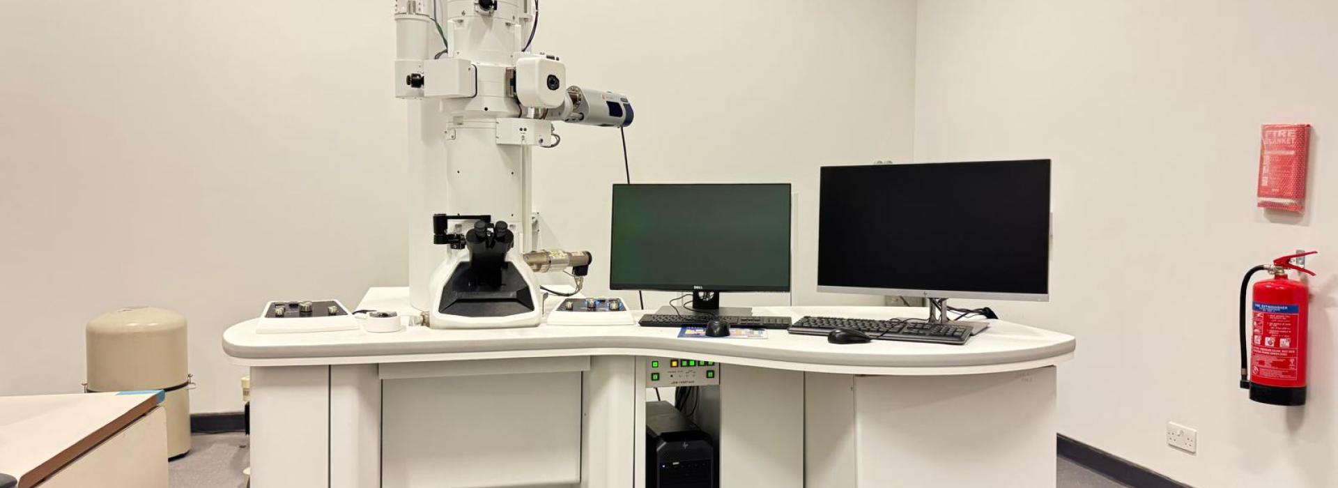
Transmission Electron Microscope
Our advanced JEOL JEM-1400 Flash TEM, integrated with the Oxford Instruments Xplore EDS system, offers unparalleled capabilities for deep nanoscale analysis. Our expert technicians ensure optimal data through meticulous sample preparation and proficient instrument operation, leveraging diverse capabilities:
- Advanced Imaging: From fundamental Bright-Field/Dark-Field to STEM with HAADF and ABF for atomic-scale detail, utilizing high-sensitivity sCMOS/Direct Electron Detectors.
- Comprehensive Analytics: Beyond EDS for elemental mapping, we use EELS for light element composition, chemical bonding, and electronic structure, alongside Diffraction for crystal analysis.
- Specialized Sample Holders: Includes double-tilt for 3D tomography, cryo-TEM for sensitive samples, and heating, tensile/straining, or electrical feedthrough holders for in-situ experiments.
- Enhanced Software: Advanced tools for tomography, CLEM, automated acquisition, and drift correction ensure high-fidelity data.
We provide accurate and robust data sets essential for your research. Explore our comprehensive results Here. To discuss collaborative projects or request specialized analyses, please complete our application form Here.
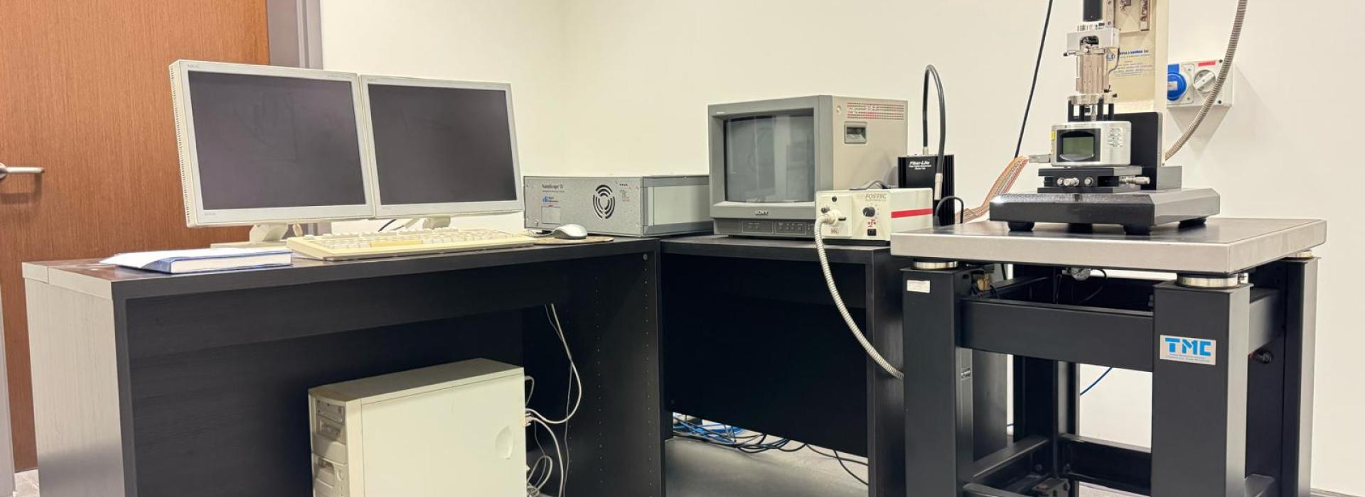
Atomic Force Microscope
Our Bruker MultiMode-1788EX Nanoscope 492 Atomic Force Microscope (AFM) is optimized for precise nanoscale surface analysis and quantitative mechanical property mapping. Key operational characteristics include:
- Sub-Nanometer Vertical Resolution: Facilitates high-precision three-dimensional topographical mapping, resolving minute features on sample surfaces.
- Diverse Imaging Modalities: Incorporates fundamental modes such as Contact Mode and Intermittent Contact Mode (TappingMode™) for robust topographical imaging, along with Phase Imaging for material property differentiation.
- Quantitative Nanomechanical Analysis: Performs Force Spectroscopy to derive quantitative measurements of surface mechanics, including adhesion forces, elastic modulus, and material stiffness.
- Environmental Versatility: Capable of high-resolution operation in both ambient air and various liquid environments, accommodating a broad spectrum of sample types and experimental conditions.
We provide accurate and robust data sets essential for your research. Explore our comprehensive results Here. To discuss collaborative projects or request specialized analyses, please complete our application form Here.


 الملون
 تدرج الرمادي


